

Australian startup Syenta has secured $26 million in Series A funding to commercialise a new manufacturing approach aimed to tackle a growing constraint in the global semiconductor supply chain.
The round was led by Playground Global and Australia’s National Reconstruction Fund, with additional backing from Investible, Salus Ventures, Jelix Ventures and Wollemi Capital. The latest raise brings Syenta’s total funding to A$51.1 million (approximately US$36.4 million), underscoring growing investor confidence in its technology.
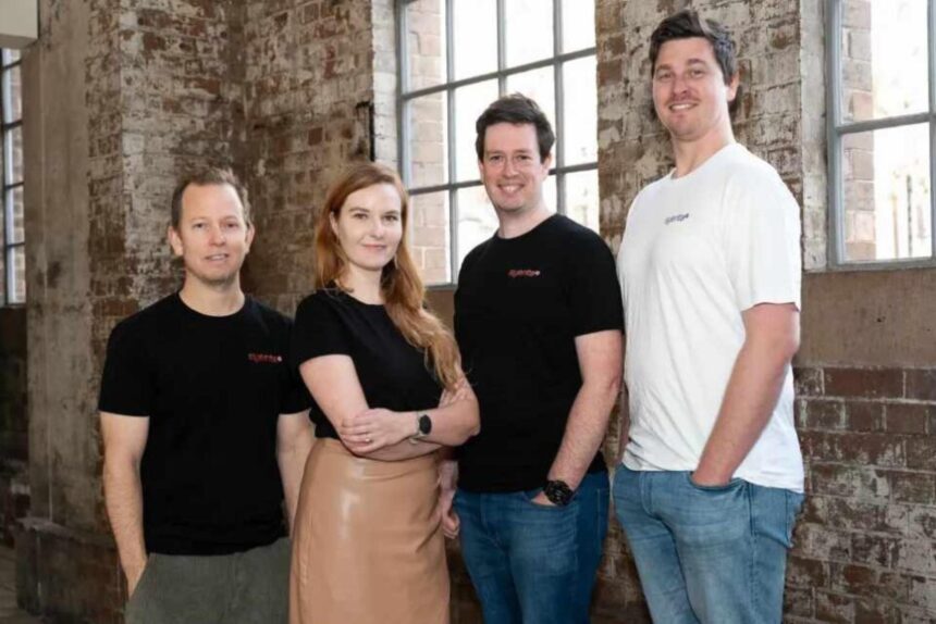
“We’re enabling finer-pitch connections within existing manufacturing infrastructure, allowing systems to move more data more efficiently and at a lower cost without requiring entirely new fabrication approaches,” said Dr. Jekaterina Viktorova, CEO and founder of Syenta.
As part of the deal, former Intel chief executive Pat Gelsinger, now a general partner at Playground Global will join the company’s board.
What you need to know
Syenta also plans to establish a US office in Arizona, positioning itself close to major semiconductor fabrication hubs operated by Intel and Taiwan Semiconductor Manufacturing Company (TSMC).
The semiconductor industry is undergoing a structural shift. Leading AI chips from companies such as Nvidia and Google are no longer built as single monolithic units. Instead, they are composed of multiple “chiplets” that must be interconnected with extreme precision.
This evolution has made advanced packaging a critical step in the production process, and a major constraint.
Currently, much of this work is dominated by TSMC, whose advanced packaging capabilities have become a key bottleneck in the global AI supply chain. Limited interconnect density and complex fabrication requirements are restricting how quickly manufacturers can scale production.
A different approach to chip assembly
At the core of Syenta’s proposition is a rethink of how chip interconnects are manufactured.
Traditional methods rely on constructing a base layer, effectively a large, complex substrate through time-intensive fabrication processes. This stage adds cost and slows production.
Syenta’s alternative uses an electrochemical technique that deposits copper wiring directly onto the base layer, akin to a high-precision stamping process. The company says this reduces manufacturing steps by around 40 per cent and eliminates the need for specialised equipment.
Crucially, it also cuts production time dramatically.
Speed, scale and supply chain implications
The potential impact extends beyond manufacturing efficiency.
By accelerating the production of base layers, Syenta’s method could allow more chips to move through the packaging stage, alleviating one of the less visible constraints on AI system deployment.
In effect, faster packaging could translate directly into faster scaling of AI infrastructure, a critical advantage as demand from data centres and enterprise applications continues to surge.
Looking ahead to commercial scale
Syenta is already collaborating with several chip designers and is targeting high-volume production by 2028, signalling a medium-term bet on sustained demand for advanced packaging solutions.
Its expansion into the United States also reflects the geographic realignment of semiconductor manufacturing, as governments and companies invest heavily in domestic capacity.
The company’s core thesis is that the next leap in AI performance may not come from making chips more powerful, but from connecting them more efficiently.
Experts say if Syenta’s approach proves scalable, it could help unlock a new phase of AI growth, easing supply chain pressures and enabling faster deployment of increasingly complex systems.
Talking Points
It is striking that Syenta is not trying to outcompete on chip design, but instead targeting a less visible constraint in the AI value chain: packaging. This reflects a deeper shift in the industry, where performance gains are increasingly limited not by compute, but by how chips are integrated.
By focusing on interconnect density and manufacturing efficiency, Syenta is addressing one of the most critical bottlenecks in scaling AI systems today. This positions the company not just as a hardware innovator, but as a potential enabler of broader supply chain resilience.
At Techparley, we see this as part of a wider evolution in semiconductors, where system-level optimisation is becoming just as important as advances in silicon itself. The companies that unlock efficiency at this layer could shape the next phase of AI growth.
The promise of reducing production time from hours to minutes is particularly significant. If scalable, this could materially increase throughput across the packaging stage, easing pressure on a supply chain currently dominated by a handful of players.
Syenta’s decision to expand into Arizona suggests a clear understanding of where influence and opportunity lie, placing the company closer to leading fabrication hubs and potential customers.
——————-
Bookmark Techparley.com for the most insightful technology news from the African continent.
Follow us on Twitter @Techparleynews, on Facebook at Techparley Africa, on LinkedIn at Techparley Africa, or on Instagram at Techparleynews.